Schematic driven PCB design
The requirements on CAD systems for IC design are much higher than for PCB design. So things good enough for the first are by far good enough for the second. The LayoutEditor offers any feature to design intricate PCBs. This tutorial explains how.
External Schematic/Netlist
 Beside the usage of the integrated schematic the LayoutEditor works together with many popular programs. It supports common netlist formats like Spice, Pads-pcb, qucs or Alliance format. The correct operation had been test with several programs like LT-Spice, DesignWorks or QUCS. The LayoutEditor works with both flat and hierarchical netlists. Also a combinated design PCB and LTCC, SAW, thin film, COB, ... is possible.
Setting up for PCB
 The LayoutEditor includes some macros doing the layer setup for PCB designs. The setup macros are located in the menu at: Utilities/Macros/PCB/X layer PCB setup. Micro and blind vias are supported, but disabled in the standard setups. Uncomment the corresponding sections in the setup macro to enable it. Adjust any settings to the design rules of your PCB manufacturer.
Beside the layer setup, a setup of a library had to be done. The library performs a link between the devices in the netlists and the pin layout on the PCB. The LayoutEditor includes library templates and a base library with common packages. These libraries/templates are located in the folder library and library/pcb. Import or add the device you need for your PCB. The libraries discretes and transitors are good templates to do so. If you import the netlist direct without using the integrated SchematicEditor the library file pcb.lel is a good template for a import library. Add required libraries (Utilities/Netlist Tools/AddLibrary) to the library list before opening the netlist.
Designing the PCB
 Actually this was already the PCB specific part of the design. Now you can layout and check the PCB as described in Netlist driven layout with LVS. Some additional macros simplyfing the PCB design are also shipped with the LayoutEditor and are located next to the PCB setup macros.
PCB 3D Display
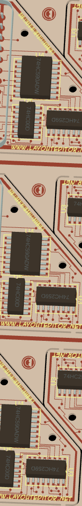
 The library shipped with the LayoutEditor includes a 3d view of the packages. To use the 3d view open a new window, load the cross-section file of the library and setup the 3d view with your pcb layer setup cell. Some PCB examples designed with the LayoutEditor are included in any package. The design shown on this pages is the "controller" example.

